I finally made my own induction heater with no protection! [Edit] Added new soft-start circuit at the end of article.
Well, I had to cut a bunch of clips to simplify the video and make it more digestible! But if you are interested to watch the cut scenes, here they are:
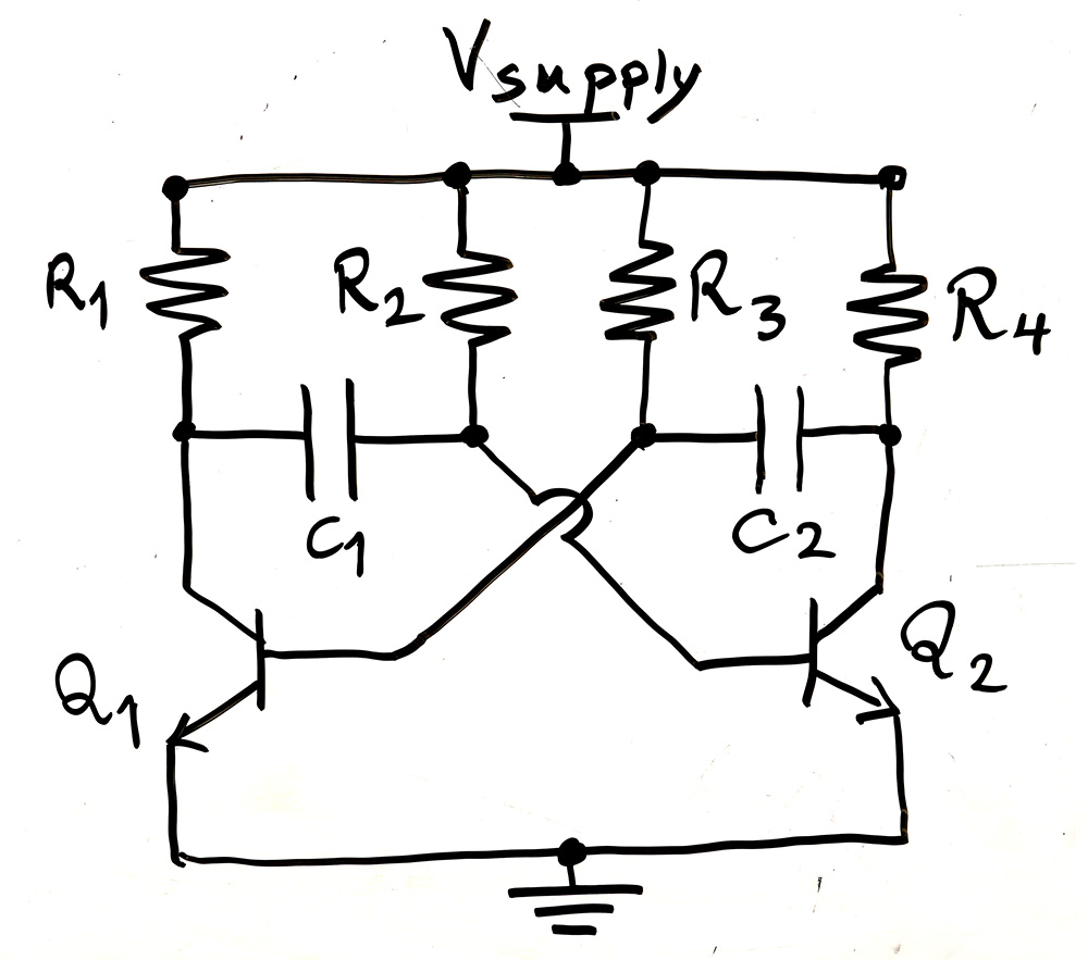
Now let’s explain the circuit I used. From what I found over the web, this specific circuit is credited to Vladimiro Mazzilli which as I explained in the video is a variation of the famous Astable Multi-Vibrator circuit shown below:
Of course the more famous vibrator circuit is done by BJT transistors shown below which works the same way. In both cases, the time it takes to charge the capacitors through the surrounding resistors defines the oscillating frequency. If you have different capacitors or resistor on each side, you can change the duty cycle.
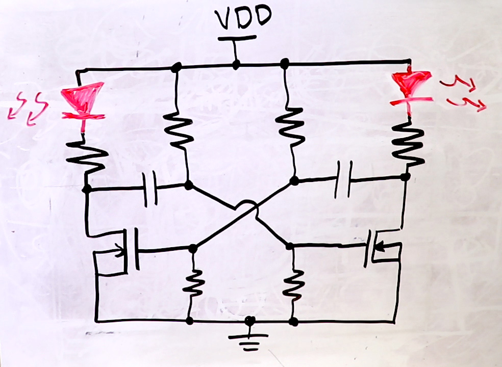
Let’s focus on the ZVS circuit. It doesn’t take much for an inductor and a capacitor put together to oscillate! Just fling the circuit and it goes BOAOAOA! Well this circuit is not the final version I put together.
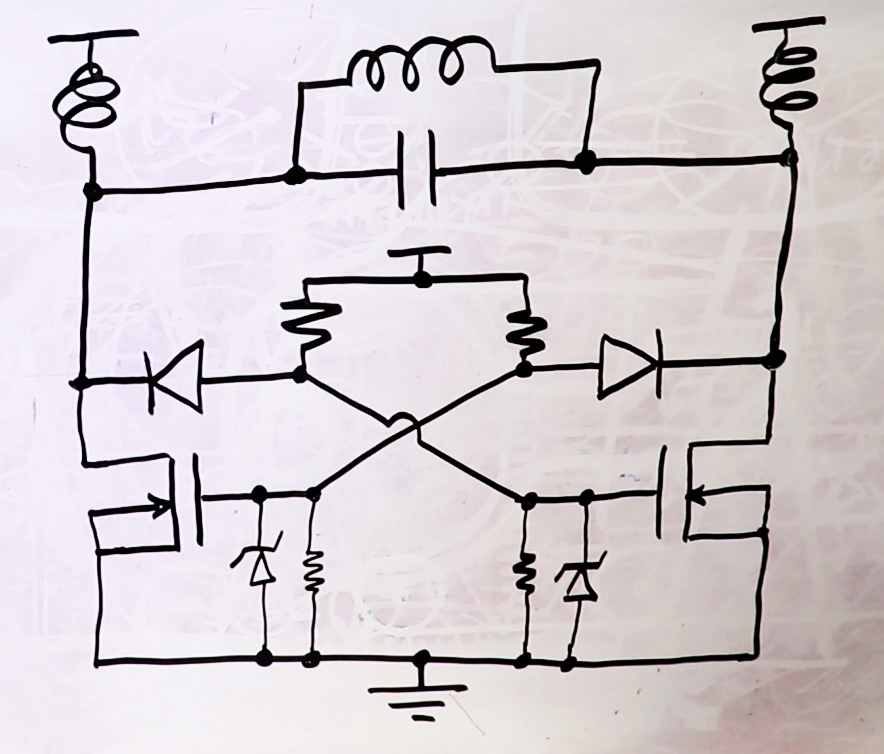
The circuit I put together looks more like the one below. Now if you can give me your time, I shall explain!!
STILL… I don’t like this circuit as is. See a major problem with this circuit is that the supply voltage must rise fast. Like I have to connect it to a battery directly or make sure my lab supply is on and then connect it. This is because otherwise if the supply voltage rises slowly, the kick to the LC circuit that makes it resonate won’t be great enough and the initial resonating voltages will be small and won’t switch transistors and dies away. In this case both gate voltages rise, turning both transistors on constantly and basically short the supply or battery and the result would be BURN!! So if for example you try to clean the supply voltage by a large capacitor, which I tried with bad results, the supply rises slowly and causes the same problem and circuit burns.
So, what was my criteria to design this circuit? First things first, I knew I would potentially need a ton of current when heating. You noticed in the video I drew over 17 amps. I picked a 12V supply so I could use my battery that could deliver more than my desk power supplies could.
Of course the other way to reduce current is to raise voltage, like they do with real induction cooker ovens. But then it is more challenging to design for higher voltages without… you know… getting shocked in every turn and potentially fail!!
So at 12V I decided to handle a few 100 watts, not to draw super huge amounts of currents either! Well my criteria is in my hands really, I’m the only customer, DEAL WITH IT!!
I thought the 20kHz the regular induction cookers use is a good compromise for this circuit. Higher frequencies could be better to reduce required inductance and capacitances for the same impedance as I mentioned, but that poses another problem:
The transistors in this circuit are not driven properly. YES I SAID IT! They are driven poorly. A MOSFET gate needs to be driven quite strong for super fast switching. That’s why there are MOSFET drivers that can handle 1A or above driving the MOSFET gate.
“But Mehdi, MOSFET Gate doesn’t draw current…”, go ahead and slap yourself across the face! MOSFET gate has an input capacitance, which means in order to change gate voltage you have to pour current into it to charge and discharge it and the more current, the faster the rate of change.
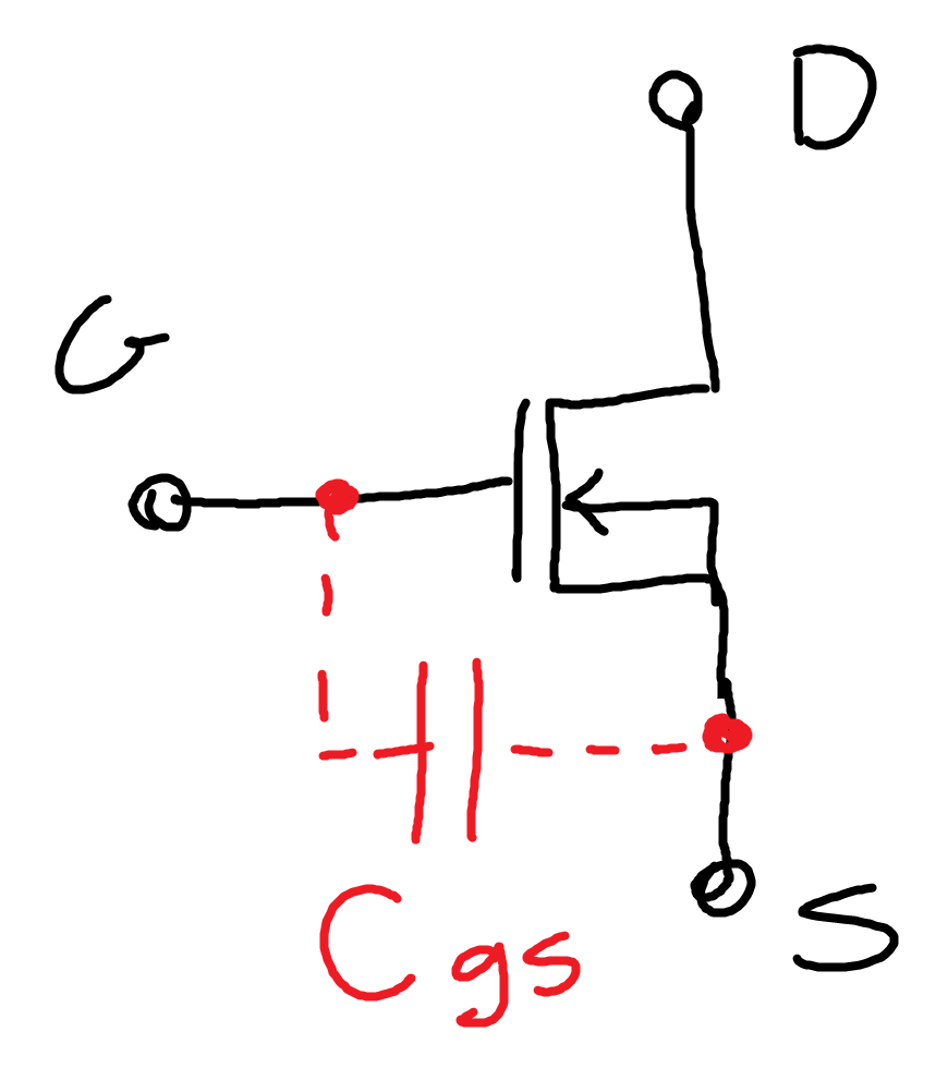
The main issue with powerful high current transistors is that they also have larger gate-source capacitances shown below (10nF in my case) and so need stronger drives.
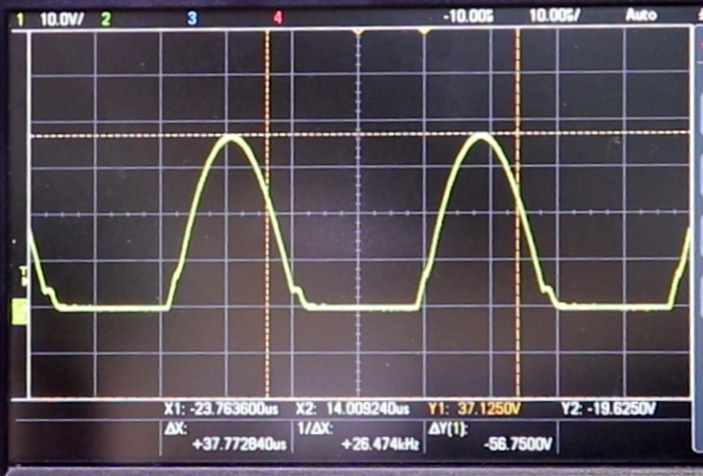
But in this circuit the gate is pulled up with resistors and lowered at the relatively slow pace of the oscillating sinewave shown below. You can clearly see where the MOSFET is switching in those flat areas at the lower voltages. Why do those flat areas happen? Read on!
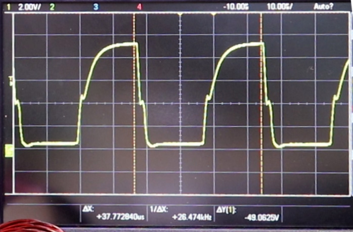
And below is the gate voltage. The rise time is dictated by the input capacitance of the MOSFET (Cgs) and the pull up resistor, which is not very fast, and the faster fall time is due to faster and stronger dropping resonance voltage showed above. But that’s not all, you see flat areas here too at around 4V that is the MOSFET VGS threshold voltage, which is due another internal transistor capacitances, namely drain-gate capacitance.
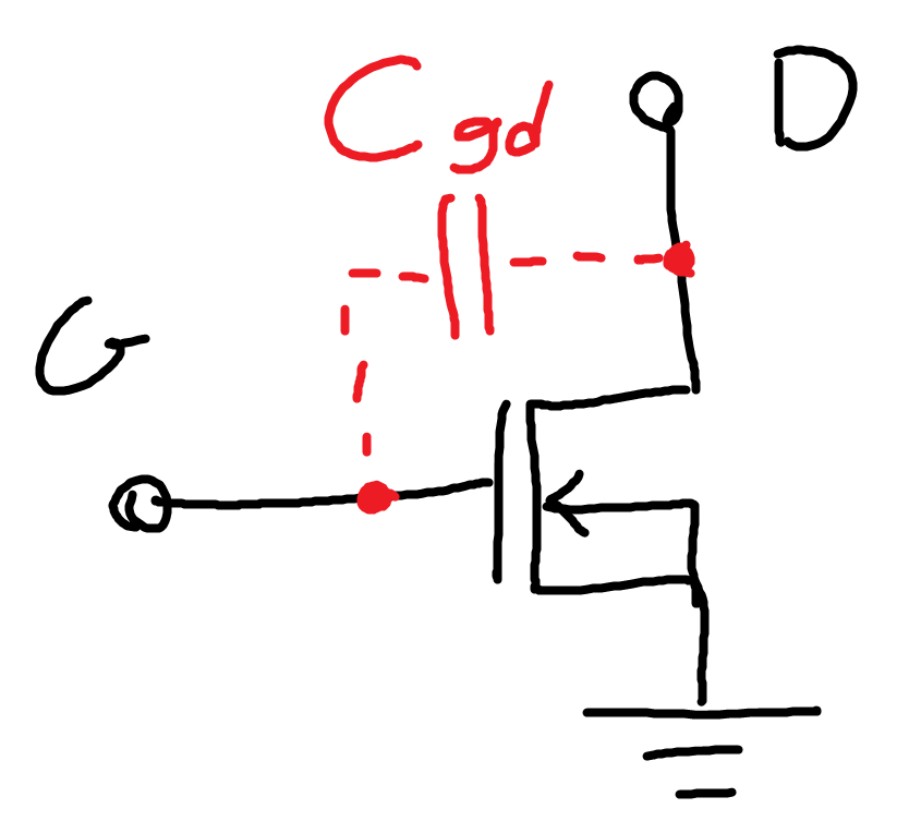
Below I show this internal capacitance as Cgd. When the drain of the transistor switches and the drain voltage changes rapidly, that fast change through Cgd creates a negative feedback to the gate and won’t allow the gate voltage to change easily as long as the drain voltage is switching, hence creating a flat voltage area around the threshold voltage when the transistor is switching and drain voltage is changing fast.
So the total switching time is greatly affected by both Cgs and Cgd. The slow switching speed means the transistor spends a relatively long time in transition period when the Drain-Source resistance is switching from a relative short circuit to open circuit. If the resistance is zero or infinite, for a limited voltages and currents there is no power wasted. But during switching with non-zero resistance, while the transistor is switching high currents too, large power is wasted over the transistor heating it up. That’s why transistor needs a proper gate drive to switch fast and shorten this transition period to lower power consumption, cooler transistors and higher efficiency.
In any case, a higher resonance frequency would also mean the switching period would be a larger portion of the cycle, wasting even more energy on transistors heating them much higher. 20KHz is a good frequency to keep power low. But any lower, you go into human hearing range and hear buzzing, not to mention inductors and capacitors must be bigger.
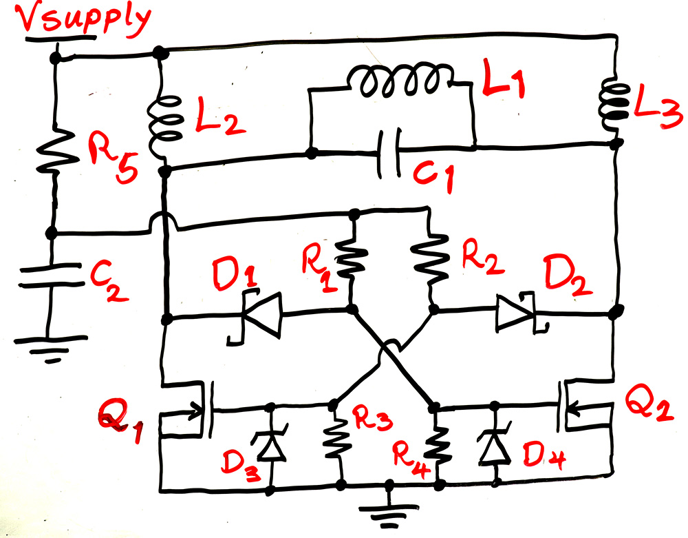
You might say, at least for pull up resistors, make them small to allow larger currents and reduce rise time. WELL I DID! They are 165 ohms now and still not fast enough. Remember when the transistor is off and gate voltage is low, those resistors fall between the 12V supply and get hot quick. Again, the proper way is a powerful gate driver, like MIC4452YN or similar.
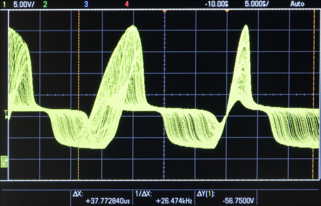
And one more thing, the switching transistors put a massive noise on the power supply as you see in the picture below, especially at higher load current. Considering in the original circuit the gate pull-up resistors are connected to the supply, this noise would create a feedback to the gate causing unwanted oscillations, slowing down switching and other issues. That’s why in my circuit I added R5 and C2 to supply the pull up resistors, so that the voltage is filtered and clean during switching.
Now, D3 and D4 zener diodes are good to keep the gate voltage below a safe level. But since we picked the supply at 12V they should be save without. But then what if switching or other noises get into gate voltage and raise it for no good intentions? Let’s keep those zeners in! R3 and R4 are not necessary though, we have enough much stronger resistors there to pull gate around!
D1 and D2 need to be fast, so I picked some Schottky diodes.
And for the massive 10uH inductor, WE NEED THICK WIRES! I didn’t have thick wires! I used some 18AWG magnet wire and made it three strands to handle more current and used an online calculator to design an inductor with air core:
https://www.allaboutcircuits.com/tools/coil-inductance-calculator/
Yet, L1 inductor is handling a ton of current, 30A peak or ~21A RMS in my case. And I measured my coil resistance is around 15mOhm, which means P = R x I^2 = 6.6 Watts is wasted over the coil itself heating it easily! That’s why having a fan to keep the circuit down is good and why my supply current is not zero at no load, lowering the efficiency. We need thicker wires, which would reduce unwanted waste and lower supply idle current.
For L2 and L3 I didn’t find something that could handle so high of a current and high enough inductance and maybe for good reason! So I decided to find a suitable inductor core and wind my own inductor! The core has AL = 10.8uH, which means one turn of wire creates 10.8uH. And Total inductance is AL x n^2, and n is the number of turns. So 4 turns would provide around 172uH. I used double wires to handle the current better.
But then I hit a problem. It seems my core get’s saturated easily at the currents I need. What does it mean to saturate? It means when there is too strong magnetic fields that fully magnetize the core, the core won’t be effective for more magnetic fields because it doesn’t magnetize any further. This means the core is weaker at higher currents and the inductance drops .
AND THAT’s the problem I observed. At no load when L2 and L3 currents were low I had 20kHz. But when I added some load, I noticed the frequency went up as high as 50kHz, AND the current from supply significantly rose. This was because reduced L2 and L3 that are paralleled with L1 reduced the total inductance and rose the resonance frequency, and couldn’t filter current effectively either.
So I ended up putting two of them in series for each inductor to keep the inductance high! I could reduce 4 turns to 3 on each core to lower the chance of saturation too. Anyway I ended up with this:
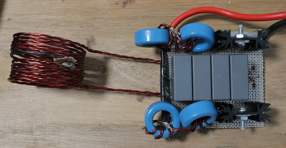
So, let me list you all the components I used:
- L1: 12 turns, ~5cm diameter and ~3.5cm length, air core
- L2 and L3 core: EPCOS/TDK B64290L0618X038
- C1, 4x capacitors in parallel: Kemet R76IR415050H3J
- C2: 10uF 16V Electrolytic
- R1 and R2: 165 Ohm 250mW
- R3 and R4 (if you use them): 10kOhm
- R5: 47 Ohm
- D1 and D2: On-Semi BZX79C15-T50R
- D3 and D4: On-Semi SB1100
- Q1 and Q2: Infineon IRFB7534PBF
- Heatsinks (use thermal grease): CUI Devices HSE-B20254-035H-02
And… there you have it! have fun!
Soft-Start Circuit
As I mentioned in my new video about making high voltage using this ZVS circuit, I added a simple circuit shown below to soft-start the ZVS.
It is not by any means a sufficient soft start, but at least with this circuit the main ZVS won’t turn on right away while the supply is rising slowly or fluctuating which could be pretty damaging to the ZVS. When ZVS turns on, it could draw double the amount of current through the LC circuit, which is already above 30A! Also if the supply rises slowly, the circuit may not oscillate at all, but will short circuit the power supply. So those early moments are very important.
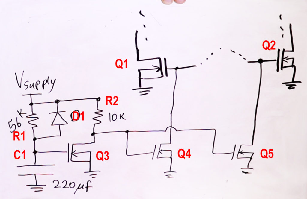
In the above circuit, Q1 and Q2 are the main ZVS transistors that oscillate at resonance of the main LC components. What I like to do is to keep them off for a few seconds after power up, and that’s where the rest of the circuit comes in. When Vsupply jumps up, C1 capacitor voltage initially remains at zero and charges slowly by R1. This keeps Q3 gate low keeping it off, and so its drain voltage is pulled up by R2 which is also Q4 and Q5 gate voltages. So, Q4 and Q5 are on, pulling Q1 and Q2 gate voltages down keeping them off.
As C1 is slowly charging through R1, eventually Q3 gate reaches the transistor threshold voltage turning Q3 on, pulling both Q4 and Q5 gates low turning them off, releasing Q1 and Q2 gates allowing them to start to oscillate.
What D1 does is kind of important. See, without D1 if you unplug the circuit, C1 voltage doesn’t drop quickly and if you plug it right back the soft start won’t work because C1 is already charged. But with D1 added, unplugging the circuit, as Vsupply drops rapidly under load, D1 will quickly pull C1 voltage down discharging it. So every time you plug the circuit in there is sure to be soft start function.
And of course adjusting R1 and C1 values you can choose the amount of on-time you like. The transistors I used for Q3, Q4 and Q5 are just some generic ones, 2N7000 or similar.
SIMPLE AS THAT!